technical ceramic solutions

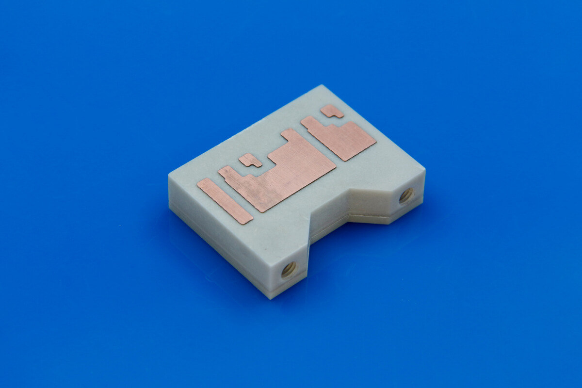
AMB for new generation semiconductor

When perform brazing (for example, Ag) in the H2 environment and it requires extreme heat and energy cycle resistance, with unique high and low temperature impact resistance, AMB substrates become an ideal packaging material for new generation semiconductor (SIC) and new high power electronic devices, it retains good thermal stability even beyond 1000 cycles.

The copper thickness is 0.1-0.5mm, provides very high ampacity and very good heat spreading. This makes it a preferred material for the applications:
-IGBT
-Power Modules
-Automotive Power Electronics
-Renewable Energy
-Space and Industrial
-Others
Aluminum Nitride AMB

Aluminum Nitride AMB


Related Products

  • Alumina Ceramic Focus Rings

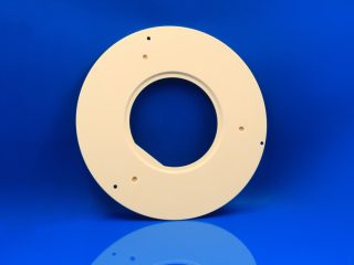
    Alumina Ceramic Focus Rings

    Alumina Ceramic Focus rings are designed to improve etch uniformity around the wafer edge or perimeter. When used with an electrostatic chuck (e-chuck), the wafer rests on the edge focus ring - held i…

  • BMA Boron Nitride Atomization Nozzles

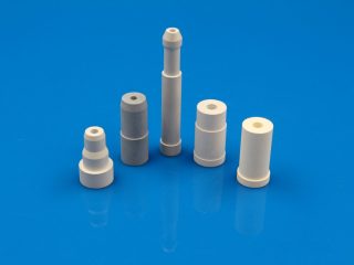
    BMA Boron Nitride Atomization Nozzles

    Innovacera's BMA boron nitride composite nozzles deliver superior precision and reliability in molten metal atomization, so Innovacera BMA boron nitride nozzles is precision atomization for molten met…

  • Petroleum pressure-bearing connector

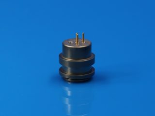
    Petroleum pressure-bearing connector

    Petroleum pressure-bearing connectors mainly rely on glass/ceramic-metal sealing technology to achieve high telecommunication transmission and pressure-bearing performance under high temperature and h…

Enquiry